 | –≠–ª–µ–∫—Ç—Ä–æ–Ω–Ω—ã–π –∫–æ–º–ø–æ–Ω–µ–Ω—Ç: SP6134HEU | –°–∫–∞—á–∞—Ç—å:  PDF PDF  ZIP ZIP |

1
Date: 8/4/04
SP6134H High Voltage, 600KHz Synchronous PWM Controller © Copyright 2004 Sipex Corporation
SP6134H
FEATURES
3V to 28V Step Down Achieved Using Dual Input
Small 10-Pin MSOP Package
2A to 15A Ouput Capability
Highly Integrated Design, Minimal Components
UVLO Detects Both V
CC
and V
IN
Short Circuit Protection with Auto-Restart
On-Board 1.5 sink (2 source) NFET Drivers
Programmable Soft Start
Fast Transient Response
High Efficiency: Greater than 94% Possible
A Synchronous Start-Up into a Pre-Charged Output
High Voltage, 600 KHz Synchronous PWM Controller
DESCRIPTION
The SP6134H is a high voltage, synchronous step-down switching regulator controller optimized for high efficiency.
The part is designed to be especially attractive for dual supply, 12V step down with 5V used to power the controller.
This lower V
CC
voltage minimizes power dissipation in the part. The SP6134H is designed to drive a pair of external
NFETs using a fixed 600kHz frequency, PWM voltage mode architecture. Protection features include UVLO, thermal
shutdown and output short circuit protection. The SP6134H is available in the cost and space saving 10-pin MSOP
.
Æ
Preliminary
TYPICAL APPLICATION CIRCUIT
APPLICATIONS
Wireless Base Station
Automotive
Industrial
Power Supply
V
CC
GL
GND
V
FB
COMP
SP6134H
10 Pin MSOP
1
2
3
4
5
10
9
8
7
6
BST
GH
SWN
SS
UVIN
8 7 6 5
1 2 3
4
CSS
47nF
CBST
1µF
FDS6676S
14.5A, 6.0m
C3
47µF
6.3V
R1
68.1k, 1%
V
OUT
VIN
0.8V - 3.3V
0 - 10 A
R2
21.5k, 1%
C
VCC
10µF
6.3V
R3
221k, 1%
R4
100k, 1%
CF1
100pF
CZ2
820pF
CP1
56pF
fs=600Khz
RZ2
40.2k, 1%
FDS6676S
14.5A, 6m
8 7 6 5
4
1 2 3
DBST
MBR0530
SP6134H
1
2
3
4
5
10
9
8
7
6
VCC
GL
GND
VFB
COMP
BST
GH
SWN
SS
UVIN
UV
IN
V
CC
GND 3
RLF
3.0,5%
U1
C
VCC
Ceramic
8050
X5R
QT
SS
GND2
C3, C4
Ceramic
1210
X5R
C4
47µF
6.3V
RZ3
4.64k, 1%
CZ3
220pF
C1
22µF
16V
C2
22µF
16V
GND
VIN
3.5V - 15V
C1, C2
Ceramic
1210
X5R
V
OUT
=(R1/R2 +1)V
FB
R5
Bead
QB
= 5V @ 30mA
0.8V
Now Available in Lead Free Packaging

2
Date: 8/4/04
SP6134H High Voltage, 600KHz Synchronous PWM Controller © Copyright 2004 Sipex Corporation
PARAMETER
MIN
TYP
MAX
UNITS
CONDITIONS
QUIESCENT CURRENT
V
CC
Supply Current
1.5
3
mA
V
FB
=0.9V (No switching)
BST Supply Current
0.2
0.4
mA
V
FB
=0.9V (No switching)
PROTECTION: UVLO
V
CC
UVLO Start Threshold
4.00
4.25
4.5
V
V
CC
UVLO Stop Threshold
3.80
4.05
4.4
V
V
CC
UVLO Hysteresis
100
200
300
mV
UVIN Start Threshold
2.3
2.5
2.65
V
UVIN Stop Threshold
2.0
2.2
2.35
V
UVIN Hysteresis
300
mV
ERROR AMPLIFIER REFERENCE
Error Amplifier Reference
0.792
0.800
0.808
V
2X Gain Config., Measure COMP/2
Error Amplifier Reference
0.788
0.800
0.812
V
Over Line and Temperature
Error Amplifier Transconductance
6
ms
Error Amplifier Gain
60
dB
No Load
COMP Sink Current
150
µA
V
FB
= 0.9V, COMP = 0.9V
COMP Source Current
150
µA
V
FB
= 0.7V, COMP = 2.2V
V
FB
Input Bias Current
50
200
nA
V
FB
= 0.8V
Internal Pole
4
MHz
COMP Clamp
2.5
V
V
FB
=0.7V, T
A
= 25∞C
COMP Clamp Temp. Coefficient
-2
mV/∞C
CONTROL LOOP: PWM COMPARATOR, RAMP & LOOP DELAY PATH
Ramp Amplitude
0.92
1.1
1.28
V
RAMP Offset
1.1
V
T
A
= 25∞C, RAMP COMP
until GH starts switching
RAMP Offset Temp. Coefficient
-2
mV/∞C
GH Minimum Pulse Width
90
180
ns
Maximum Controllable Duty Ratio
92
97
%
Maximum Duty Ratio Measured just
before pulse skipping begins
Maximum Duty Ratio
100
%
Valid for 20 Cycles
Internal Oscillator Frequency
540
600
660
kHz
ELECTRICAL SPECIFICATIONS
Unless otherwise specified: 0∞C < T
AMB
< 70∞C, 4.5V < V
CC
< 5.5V, BST=V
CC
,SWN = GND = 0V, UVIN = 3.0V, CV
CC
= 10µF,
C
COMP
= 0.1µF, CGH = CGL = 3.3nF, C
SS
= 50nF, Typical measured at V
CC
=5V. The denotes the specifications which
apply over the full operating temperature range, unless otherwise specified.
These are stress ratings only and functional operation of the device at
these ratings or any other above those indicated in the operation sections
of the specifications below is not implied. Exposure to absolute maximum
rating conditions for extended periods of time may affect reliability.
V
CC
.................................................................................................. 7V
BST ............................................................................................... 33V
BST-SWN ......................................................................... -0.3V to 7V
SWN ................................................................................... -1V to 15V
GH ......................................................................... -0.3V to BST+0.3V
GH-SWN ......................................................................................... 7V
All other pins .......................................................... -0.3V to V
CC
+0.3V
Peak Output Current < 10us
GH,GL ............................................................................................. 2A
Storage Temperature .................................................. -65∞C to 150∞C
Power Dissipation .......................................................................... 1W
Lead Temperature (Soldering, 10 sec) ...................................... 300∞C
ESD Rating .......................................................................... 2kV HBM
Thermal Resistance ............................................................. 41.9∞C/W
ABSOLUTE MAXIMUM RATINGS
510 600 690

3
Date: 8/4/04
SP6134H High Voltage, 600KHz Synchronous PWM Controller © Copyright 2004 Sipex Corporation
PARAMETER
MIN
TYP
MAX
UNITS
CONDITIONS
TIMERS: SOFTSTART
SS Charge Current:
10
µA
SS Discharge Current:
1
mA
Fault Present, SS = 0.2V
PROTECTION: SHORT CIRCUIT & THERMAL
Short Circuit Threshold Voltage
0.2
0.25
0.3
V
Measured V
REF
(0.8V) - V
FB
Hiccup Timeout
100
ms
V
FB
= 0V
Number of Allowable Clock Cycles
20
Cycles
V
FB
= 0.7V
at 100% Duty Cycle
Minimum GL Pulse After 20 Cycles
0.5
Cycles
V
FB
= 0.7V
Thermal Shutdown Temperature
145
∞C
Thermal Recovery Temperature
135
∞C
Thermal Hysteresis
10
∞C
OUTPUT: NFET GATE DRIVERS
GH & GL Rise Times
35
50
ns
Measured 10% to 90%
GH & GL Fall Times
30
40
ns
Measured 90% to 10%
GL to GH Non Overlap Time
45
70
ns
GH & GL Measured at 2.0V
SWN to GL Non Overlap Time
20
30
ns
Measured SWN = 100mV to GL = 2.0V
GH & GL Pull Down Resistance
50
K
Resistor Pull-Down
Driver Pull Down Resistance
1.5
1.9
Note 1
Driver Pull Up Resistance
2.5
3.0
Note 1
ELECTRICAL SPECIFICATIONS: Continued
Unless otherwise specified: 0∞C < T
AMB
< 70∞C, 4.5V < V
CC
< 5.5V, BST=V
CC
,SWN = GND = 0V, UVIN = 3.0V, CV
CC
= 10µF,
C
COMP
= 0.1µF, CGH = CGL = 3.3nF, C
SS
= 50nF, Typical measured at V
CC
=5V. The denotes the specifications which
apply over the full operating temperature range, unless otherwise specified.
Note 1: Gauranteed by design, not 100% tested.

4
Date: 8/4/04
SP6134H High Voltage, 600KHz Synchronous PWM Controller © Copyright 2004 Sipex Corporation
PIN #
PIN NAME DESCRIPTION
1
V
CC
Bias Supply Input. Connect to external 5V supply. Used to power internal circuits and
low side gate driver.
2
GL
High current driver output for the low side NFET switch. It is always low if GH is high or
during a fault. Resistor pull down ensure low state at low voltage.
3
GND
Ground Pin. The control circuitry of the IC and lower power driver are referenced to this
pin. Return separately from other ground traces to the (-) terminal of C
OUT
.
4
V
FB
Feedback Voltage and Short Circuit Detection pin. It is the inverting input of the Error
Amplifier and serves as the output voltage feedback point for the Buck Converter. The
output voltage is sensed and can be adjusted through an external resistor divider.
Whenever V
FB
drops 0.25V below the positive reference, a short circuit fault is detected
and the IC enters hiccup mode.
5
COMP
Output of the Error Amplifier. It is internally connected to the non-inverting input of the
PWM comparator. An optimal filter combination is chosen and connected to this pin and
either ground or V
FB
to stabilize the voltage mode loop.
6
UVIN
UVLO input for V
IN
voltage. Connect a resistor divider between V
IN
and UVIN to set
minimum operating voltage.
7
SS
Soft Start. Connect an external capacitor between SS and GND to set the soft start rate
based on the 10µA source current. The SS pin is held low via a 1mA (min) current during
all fault conditions.
8
SWN
Lower supply rail for the GH high-side gate driver. Connect this pin to the switching node
at the junction between the two external power MOSFET transistors.
9
GH
High current driver output for the high side NFET switch. It is always low if GL is high or
during a fault. Resistor pull down ensure low state at low voltage.
10
BST
High side driver supply pin. Connect BST to the external boost diode and capacitor as
shown in the Typical Application Circuit on page 1. High side driver is connected between
BST pin and SWN pin.
PIN DESCRIPTION

5
Date: 8/4/04
SP6134H High Voltage, 600KHz Synchronous PWM Controller © Copyright 2004 Sipex Corporation
General Overview
The SP6134H is a fixed frequency, voltage
mode, synchronous PWM controller optimized
for high efficiency. The part has been designed
to be especially attractive for split plane applica-
tions utilizing 5V to power the controller and 3V
to 12V for step down conversion.
The heart of the SP6134H is a wide bandwidth
transconductance amplifier designed to accom-
modate Type II and Type III compensation
schemes. A precision 0.8V reference present on
the positive terminal of the error amplifier per-
mits the programming of the output voltage
down to 0.8V via the V
FB
pin. The output of the
error amplifier, COMP, compared to a 1.1V
peak-to-peak ramp is responsible for trailing
edge PWM control. This voltage ramp and PWM
control logic are governed by the internal oscil-
lator that accurately sets the PWM frequency to
600kHz.
FUNCTIONAL DIAGRAM
THEORY OF OPERATION
The SP6134H contains two unique control fea-
tures that are very powerful in distributed appli-
cations. First, asynchronous driver control is
enabled during start up to prohibit the low side
NFET from pulling down the output until the
high side NFET has attempted to turn on. Sec-
ond, a 100% duty cycle timeout ensures that the
low side NFET is periodically enhanced during
extended periods at 100% duty cycle. This guar-
antees the synchronized refreshing of the BST
capacitor during very large duty ratios.
The SP6134H also contains a number of valu-
able protection features. A programmable input
(V
IN
) UVLO allows a user to set the exact value
at which the conversion voltage is at a safe point
to begin down conversion, and an internal V
CC
UVLO ensures that the controller itself has
enough voltage to properly operate. Other pro-
1.7 V
1.7 V
COMPARATOR
ASYNC. STARTUP
0.4 V
FAULT
CLR
COUNT 20
CLOCK
PULSES
600 kHZ
CLK
CLOCK PULSE GENERATOR
SS
GL HOLD OFF
100% Protection Logic
Q
R
S
RESET
DOMINANT
QPWM
CLK
SYNCHRONOUS
DRIVER
GND
3
2 GL
PWM LOOP
5 COMP
POS REF
FAULT
1
7
0.8V
CORE
REFERENCE
V
CC
FAULT
SOFTSTART INPUT
RAMP = 1.1V
VFBINT
VPOS
Gm
Gm ERROR AMPLIFIER
9 GH
8 SWN
10 BST
VFB
SS
10 µA
VCC
VCC
VCC
FAULT
REF OK
FAULT
POWER FAULT
HICCUP FAULT
REF OK
VIN UVLO
VCC UVLO
2.50 VON
2.20 V OFF
6
UVIN
4.25 V ON
4.05 V OFF
Q
VCC
REF OK
200ms Delay
COUNTER
CLR
CLK
R
SET
DOMINANT
S
+
-
THERMAL
SHUTDOWN
145 ∞C ON
135 ∞C OFF
SHORT CIRCUIT
DETECTION
VFBINT
+ -
VPOS
0.25 V
THERMAL AND SHORT CIRCUIT PROTECTION
UVLO COMPARATORS
+
-
+
-

6
Date: 8/4/04
SP6134H High Voltage, 600KHz Synchronous PWM Controller © Copyright 2004 Sipex Corporation
tection features include thermal shutdown and
short-circuit detection. In the event that either a
thermal, short-circuit, or UVLO fault is de-
tected, the SP6134H is forced into an idle state
where the output drivers are held off for a finite
period before a re-start is attempted.
Under Voltage Lock Out (UVLO)
The SP6134H contains two separate UVLO
comparators to monitor the bias (V
CC
) and con-
version (V
IN
) voltages independently. The V
CC
UVLO threshold is internally set to 4.25V,
whereas the V
IN
UVLO threshold is program-
mable through the UVIN pin. When the UVIN
pin is greater than 2.5V, the SP6134H is permit-
ted to start up pending the removal of all other
faults. Both the V
CC
and V
IN
UVLO compara-
tors have been designed with hysteresis to pre-
vent noise from resetting a fault.
Soft Start
"Soft Start" is achieved when a power converter
ramps up the output voltage while controlling
the magnitude of the input supply source cur-
rent. In a modern step down converter, ramping
up the positive terminal of the error amplifier
controls soft start. As a result, excess source
current can be defined as the current required to
charge the output capacitor.
IV
IN
= C
OUT
* DV
OUT
/ DTSoft-start
The SP6134H provides the user with the option
to program the soft start rate by tying a capacitor
from the SS pin to GND. The selection of this
capacitor is based on the 10uA pull up current
present at the SS pin and the 0.8V reference
voltage. Therefore, the excess source can be
redefined as:
IV
IN
= C
OUT
* DV
OUT
*10
µA / (C
SS
* 0.8V)
Hiccup
Upon the detection of a power, thermal, or short-
circuit fault, the SP6134H is forced into an idle
state for 100mS (typical). The SS and COMP
pins are immediately pulled low, and the gate
drivers are held off for the duration of the
timeout period. Power and thermal faults have
to be removed before a restart may be attempted,
whereas, a short-circuit fault is internally cleared
shortly after the fault latch is set. Therefore, a
restart attempt is guaranteed every 100mS (typi-
cal) as long as the short-circuit condition per-
sists.
Thermal and Short-Circuit
Protection
Because the SP6134H is designed to drive large
NFETs running at high current, there is a chance
that either the controller or power converter will
become too hot. Therefore, an internal thermal
shutdown (145
∞C) has been included to prevent
the IC from malfunctioning at extreme tempera-
tures.
A short-circuit detection comparator has also
been included in the SP6134H to protect against
the accidental short or sever build up of current
at the output of the power converter. This com-
parator constantly monitors the positive and
negative terminals of the error amplifier, and if
the V
FB
pin ever falls more than 250mV (typi-
cal) below the positive reference, a short-circuit
fault is set. Because the SS pin overrides the
internal 0.8V reference during soft start, the
SP6134H is capable of detecting short-circuit
faults throughout the duration of soft start as
well as in regular operation.
Error Amplifier and Voltage Loop
As stated before, the heart of the SP6134H
voltage error loop is a high performance, wide
bandwidth transconductance amplifier. Because
of the amplifier's current limited (+/-150
µA)
transconductance, there are many ways to com-
pensate the voltage loop or to control the COMP
pin externally. If a simple, single pole, single
THEORY OF OPERATION: Continued
7
Date: 8/4/04
SP6134H High Voltage, 600KHz Synchronous PWM Controller © Copyright 2004 Sipex Corporation
THEORY OF OPERATION: Continued
zero response is required, then compensation
can be a simple as an RC to ground. If a more
complex compensation is required, then the
amplifier has enough bandwidth (45
∞ at 4 MHz)
and enough gain (60dB) to run Type III compen-
sation schemes with adequate gain and phase
margins at cross over frequencies greater than
50kHz.
The common mode output of the error amplifier
is 0.9V to 2.2V. Therefore, the PWM voltage
ramp has been set between 1.1V and 2.2V to
ensure proper 0% to 100% duty cycle capability.
The voltage loop also includes two other very
important features. One is an asynchronous start
up mode. Basically, the GL driver can not turn
on unless the GH driver has attempted to turn on
or the SS pin has exceeded 1.7V. This feature
prevents the controller from "dragging down"
the output voltage during startup or in fault
modes. The second feature is a 100% duty cycle
timeout that ensures synchronized refreshing of
the BST capacitor at very high duty ratios. In the
event that the GH driver is on for 20 continuous
clock cycles, a reset is given to the PWM flip
flop half way through the 21st cycle. This forces
GL to rise for the remainder of the cycle, in turn
refreshing the BST capacitor.
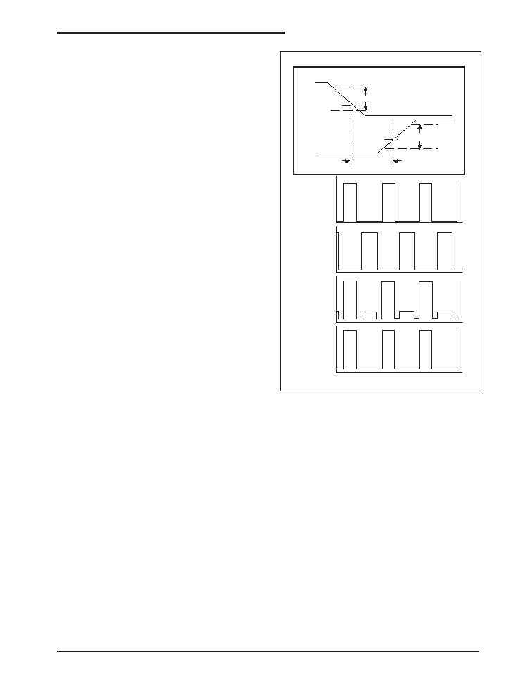
Gate Drivers
The SP6134H contains a pair of powerful 2
SOURCE and 1.5
SINK drivers. These state
of the art drivers are designed to drive external
NFETs capable of handling up to 30A. Rise,
fall, and non-overlap times have all been minized
to achieve maximum efficiency. All drive pins
GH, GL & SWN are monitored continuously to
ensure that only one external NFET is ever on at
any given time.
90%
10%
RISE TIME
2V
NON-OVERLAP
FALL TIME
2V
90%
10%
GH(GL)
GL(GH)
GATE DRIVER TEST CONDITIONS
V(BST)
GH
Voltage
V(VCC)
V(SWN)
GL
Voltage
V(VIN)
0V
-0V
-V(Diode) V
V(VIN)+V(VCC)
BST
Voltage
V(VCC)
TIME
SWN
Voltage

8
Date: 8/4/04
SP6134H High Voltage, 600KHz Synchronous PWM Controller © Copyright 2004 Sipex Corporation
APPLICATIONS INFORMATION
Inductor Selection
There are many factors to consider in selecting
the inductor including cost, efficiency, size and
EMI. In a typical SP6134H circuit, the inductor
is chosen primarily for value, saturation current
and DC resistance. Increasing the inductor value
will decrease output voltage ripple, but degrade
transient response. Low inductor values provide
the smallest size, but cause large ripple currents,
poor efficiency and more output capacitance to
smooth out the larger ripple current. The induc-
tor must also be able to handle the peak current
at the switching frequency without saturating,
and the copper resistance in the winding should
be kept as low as possible to minimize resistive
power loss. A good compromise between size,
loss and cost is to set the inductor ripple current
to be within 20% to 40% of the maximum output
current.
The switching frequency and the inductor oper-
ating point determine the inductor value as fol-
lows:
( max)
(max )
(max)
)
(
OUT
r
S
IN
OUT
IN
OUT
I
K
F
V
V
V
V
L
-
=
where:
Fs = switching frequency
Kr = ratio of the ac inductor ripple current to the
maximum output current
The peak to peak inductor ripple current is:
L
F
V
V
V
V
I
S
I N
OUT
IN
OUT
PP
(max)
(max)
)
(
-
=
Once the required inductor value is selected, the
proper selection of core material is based on
peak inductor current and efficiency require-
ments. The core must be large enough not to
saturate at the peak inductor current
2
(max)
P P
OUT
PEAK
I
I
I
+
=
and provide low core loss at the high switching
frequency. Low cost powdered iron cores have
a gradual saturation characteristic but can intro-
duce considerable ac core loss, especially when
the inductor value is relatively low and the
ripple current is high. Ferrite materials, on the
other hand, are more expensive and have an
abrupt saturation characteristic with the induc-
tance dropping sharply when the peak design
current is exceeded. Nevertheless, they are pre-
ferred at high switching frequencies because
they present very low core loss and the design
only needs to prevent saturation. In general,
ferrite or molypermalloy materials are better
choice for all but the most cost sensitive appli-
cations.
The power dissipated in the inductor is equal to
the sum of the core and copper losses. To mini-
mize copper losses, the winding resistance needs
to be minimized, but this usually comes at the
expense of a larger inductor. Core losses have a
more significant contribution at low output cur-
rent where the copper losses are at a minimum,
and can typically be neglected at higher output
currents where the copper losses dominate. Core
loss information is usually available from the
magnetic vendor.
The copper loss in the inductor can be calculated
using the following equation:
WINDING
RMS
L
Cu
L
R
I
P
2
)
(
)
(
=
where I
L(RMS)
is the RMS inductor current that
can be calculated as follows:
I
L(RMS)
= I
OUT(max)
1 + 1
(
I
PP
)
2
3 I
OUT(max)

9
Date: 8/4/04
SP6134H High Voltage, 600KHz Synchronous PWM Controller © Copyright 2004 Sipex Corporation
Output Capacitor Selection
The required ESR (Equivalent Series Resis-
tance) and capacitance drive the selection of the
type and quantity of the output capacitors. The
ESR must be small enough that both the resis-
tive voltage deviation due to a step change in the
load current and the output ripple voltage do not
exceed the tolerance limits expected on the
output voltage. During an output load transient,
the output capacitor must supply all the addi-
tional current demanded by the load until the
SP6134CU adjusts the inductor current to the
new value.
Therefore the capacitance must be large enough
so that the output voltage is help up while the
inductor current ramps up or down to the value
corresponding to the new load current. Addi-
tionally, the ESR in the output capacitor causes
a step in the output voltage equal to the current.
Because of the fast transient response and inher-
ent 100% and 0% duty cycle capability provided
by the SP6134CU when exposed to output load
transient, the output capacitor is typically cho-
sen for ESR, not for capacitance value.
The output capacitor's ESR, combined with the
inductor ripple current, is typically the main
contributor to output voltage ripple. The maxi-
mum allowable ESR required to maintain a
specified output voltage ripple can be calculated
by:
RESR
V
OUT
I
PK-PK
where:
V
OUT
= Peak to Peak Output Voltage Ripple
I
PK-PK
= Peak to Peak Inductor Ripple Current
The total output ripple is a combination of the
ESR and the output capacitance value and can
be calculated as follows:
V
OUT
=
(
I
PP
(1 ≠ D)
)
2
+ (I
PP
R
ESR
)
2
C
OUT
F
S
where:
F
S
= Switching Frequency
D = Duty Cycle
C
OUT
= Output Capacitance Value
Input Capacitor Selection
The input capacitor should be selected for ripple
current rating, capacitance and voltage rating.
The input capacitor must meet the ripple current
requirement imposed by the switching current.
In continuous conduction mode, the source cur-
rent of the high-side MOSFET is approximately
a square wave of duty cycle V
OUT
/V
IN
. Most of
this current is supplied by the input bypass
capacitors. The RMS value of input capacitor
current is determined at the maximum output
current and under the assumption that the peak
to peak inductor ripple current is low, it is given
by:
I
CIN(rms)
= I
OUT(max)
D(1 - D)
The worse case occurs when the duty cycle D is
50% and gives an RMS current value equal to
I
OUT
/2.
Select input capacitors with adequate ripple
current rating to ensure reliable operation.
The power dissipated in the input capacitor is:
)
(
2
)
(
CIN
ESR
rms
CIN
CIN
R
I
P
=
This can become a significant part of power
losses in a converter and hurt the overall energy
transfer efficiency. The input voltage ripple
primarily depends on the input capacitor ESR
and capacitance. Ignoring the inductor ripple
current, the input voltage ripple can be deter-
mined by:
2
)
(
)
(
(max)
)
(
IN
IN
S
OUT
I N
OUT
MAX
OUT
CIN
E SR
out
IN
V
C
F
V
V
V
I
R
I
V
-
+
=
APPLICATIONS INFORMATION: Continued

10
Date: 8/4/04
SP6134H High Voltage, 600KHz Synchronous PWM Controller © Copyright 2004 Sipex Corporation
APPLICATIONS INFORMATION: Continued
The capacitor type suitable for the output capac-
itors can also be used for the input capacitors.
However, exercise extra caution when tantalum
capacitors are considered. Tantalum capacitors are
known for catastrophic failure when exposed to
surge current, and input capacitors are prone to
such surge current when power supplies are con-
nected "live" to low impedance power sources.
MOSFET Selection
The losses associated with MOSFETs can be
divided into conduction and switching losses.
Conduction losses are related to the on resistance
of MOSFETs, and increase with the load current.
Switching losses occur on each on/off transition
when the MOSFETs experience both high current
and voltage. Since the bottom MOSFET switches
current from/to a paralleled diode (either its own
body diode or a Schottky diode), the voltage across
the MOSFET is no more than 1V during switching
transition. As a result, its switching losses are
negligible. The switching losses are difficult to
quantify due to all the variables affecting turn on/
off time. However, the following equation pro-
vides an approximation on the switching losses
associated with the top MOSFET driven by
SP6134H.
S
OUT
IN
rss
S H
F
I
V
C
P
(max)
(max)
(max)
12
=
where
C
rss
= reverse transfer capacitance of the top
MOSFET
Switching losses need to be taken into account for
high switching frequency, since they are directly
proportional to switching frequency. The conduc-
tion losses associated with top and bottom
MOSFETs are determined by:
D
I
R
P
OUT
ON
DS
CH
2
(max)
)
(
(max)
=
)
1
(
2
(max )
)
(
(max )
D
I
R
P
OUT
ON
DS
CL
-
=
where
P
CH(max)
= conduction losses of the high side
MOSFET
P
CL(max)
= conduction losses of the low side
MOSFET
R
DS(ON)
= drain to source on resistance.
The total power losses of the top MOSFET are the
sum of switching and conduction losses. For syn-
chronous buck converters of efficiency over 90%,
allow no more than 4% power losses for high or
low side MOSFETs. For input voltages of 3.3V
and 5V, conduction losses often dominate switch-
ing losses. Therefore, lowering the R
DS(ON)
of the
MOSFETs always improves efficiency even
though it gives rise to higher switching losses due
to increased C
rss
.
Top and bottom MOSFETs experience unequal
conduction losses if their on time is unequal. For
applications running at large or small duty cycle, it
makes sense to use different top and bottom
MOSFETs. Alternatively, parallel multiple
MOSFETs to conduct large duty factor.
R
DS(ON)
varies greatly with the gate driver voltage.
The MOSFET vendors often specify R
DS(ON)
on
multiple gate to source voltages (V
GS
), as well as
provide typical curve of R
DS(ON)
versus V
GS
. For
5V input, use the R
DS(ON)
specified at 4.5V V
GS
. At
the time of this publication, vendors, such as
Fairchild, Siliconix and International Rectifier,
have started to specify R
DS(ON)
at V
GS
less than 3V.
This has provided necessary data for designs in
which these MOSFETs are driven with 3.3V and
made it possible to use SP6134H in 3.3V only
applications.
Thermal calculation must be conducted to ensure
the MOSFET can handle the maximum load cur-
rent. The junction temperature of the MOSFET,
determined as follows, must stay below the maxi-
mum rating.
JA
MOSFET
A
J
R
P
T
T
(max)
(max)
( max)
+
=
where
T
A(max)
= maximum ambient temperature
PMOSFET(max) = maximum power dissipa-
tion of the MOSFET
R
JA
= junction to ambient thermal resistance.
R
JA
of the device depends greatly on the board

11
Date: 8/4/04
SP6134H High Voltage, 600KHz Synchronous PWM Controller © Copyright 2004 Sipex Corporation
layout, as well as device package. Significant
thermal improvement can be achieved in the maxi-
mum power dissipation through the proper design
of copper mounting pads on the circuit board. For
example, in a SO-8 package, placing two 0.04
square inches copper pad directly under the pack-
age, without occupying additional board space,
can increase the maximum power from approxi-
mately 1 to 1.2W. For DPAK package, enlarging
the tap mounting pad to 1 square inches reduces the
R
JA from 96
∞C/W to 40∞C/W.
APPLICATIONS INFORMATION: Continued
Schottky Diode Selection
When paralleled with the bottom MOSFET, an
optional Schottky diode can improve efficiency
and reduce noises. Without this Schottky diode,
the body diode of the bottom MOSFET con-
ducts the current during the non-overlap time
when both MOSFETs are turned off. Unfortu-
nately, the body diode has high forward voltage
and reverse recovery problem. The reverse re-
covery of the body diode causes additional
switching noises when the diode turns off. The
Schottky diode alleviates these noises and addi-
tionally improves efficiency thanks to its low
forward voltage. The reverse voltage across the
diode is equal to input voltage, and the diode
must be able to handle the peak current equal to
the maximum load current.
The power dissipation of the Schottky diode is
determined by
P
DIODE
= 2V
F
I
OUT
T
NOL
F
S
where
T
NOL
= non-overlap time between GH and GL.
V
F
= forward voltage of the Schottky diode.
Loop Compensation Design
The open loop gain of the whole system can be
divided into the gain of the error amplifier,
PWM modulator, buck converter output stage,
and feedback resistor divider. In order to cross-
over at the selected frequency FCO, the gain of
the error amplifier has to compensate for the
attenuation caused by the rest of the loop at this
frequency.
(SRz2Cz2+1)(SR1Cz3+1)
(SR
ESR
C
OUT
+ 1)
[S^2LC
OUT
+S(R
ESR
+R
DC
) C
OUT
+1]
V
IN
SR1Cz2(SRz3Cz3+1)(SRz2Cp1+1)
V
RAMP_PP
V
OUT
(Volts)
+
_
V
REF
(Volts)
Notes: R
ESR
= Output Capacitor Equivalent Series Resistance.
R
DC
= Output Inductor DC Resistance.
V
RAMP_PP
= SP6132 Internal RAMP Amplitude Peak to Peak Voltage.
Condition: Cz2 >> Cp1 & R1 >> Rz3
Output Load Resistance >> R
ESR
& R
DC
R
2
V
REF
(R
1
+ R
2
)
or
V
OUT
V
FBK
(Volts)
Type III Voltage Loop
Compensation
G
AMP
(s) Gain Block
PWM Stage
G
PWM
Gain
Block
Output Stage
G
OUT
(s) Gain
Block
Voltage Feedback
G
FBK
Gain Block
SP6134H Voltage Mode Control Loop with Loop
Dynamic

12
Date: 8/4/04
SP6134H High Voltage, 600KHz Synchronous PWM Controller © Copyright 2004 Sipex Corporation
APPLICATIONS INFORMATION: Continued
The goal of loop compensation is to manipulate
loop frequency response such that its gain crosses
over 0db at a slope of -20db/dec. The first step
of compensation design is to pick the loop
crossover frequency. High crossover frequency
is desirable for fast transient response, but often
jeopardizes the system stability. Crossover fre-
quency should be higher than the ESR zero but
less than 1/5 of the switching frequency. The
ESR zero is contributed by the ESR associated
with the output capacitors and can be deter-
mined by:
Z(ESR)
=
1
2
C
OUT
R
ESR
The next step is to calculated the complex con-
jugate poles contributed by the LC output filter,
P(LC)
=
1
2
L C
OUT
Frequency
(Hz)
Error Amplify Gain
Bandwidth Product
Condition:
C22 >> CP1, R1 >> RZ3
20 Log (RZ2/R1)
Gain
(dB)
1/6.28(R22) (CZ2)
1/6.28 (R1) (CZ3)
1/6.28 (R1) (CZ2)
1/6.28 (RZ2) (CP1)
1/6.28 (RZ3) (CZ3)
Bode Plot of Type III Error Amplify Compensation.
When the output capacitors are of a Ceramic
Type, the SP6134CU Evaluation Board requires
a Type III compensation circuit to give a phase
boost of 180
∞ in order to counteract the effects of
an under damped resonance of the output filter
at the double pole frequency.
Table 1. Input and Output Stage Components Selection Charts.
INDUCTORS - SURFACE MOUNT
Inductor Specification
Inductance
Manufacturer/Part No.
Series R
I
SAT
Size
Inductor Type
Manufaturer
(uH)
m
(a)
LxW(mm)
Ht.(mm)
Website
2.7
Easy Magnet SC5018-2R7M
4.30
12.0
12.6x12.6
4.5
Shielded Ferrite Core
inter-technical.com
2.7
TDK RLF 12560T-2R7N110
4.50
12.2
12.5x12.8
6.0
Shielded Ferrite Core
tdk.com
3.3
Coilcraft DO5010P-332HC
8.60
17.0
14.7x15.2
8.0
Unshielded Ferrite Core
coilcraft.com
1.2
Easy Magnet SC5018-1R2M
1.96
20.0
12.6x12.6
4.5
Shielded Ferrite Core
inter-technical.com
1.2
Inter-Technical SC4015-1R2M
4.37
17.0
10.0x10.0
3.8
Shielded Ferrite Core
inter-technical.com
1.5
Coilcraft DO5010P-152HC
4.00
25.0
14.7x15.2
8.0
Unshielded Ferrite Core
coilcraft.com
1.9
TDK RLF 12560T-1R9N120
3.60
13.2
12.5x12.8
6.0
Shielded Ferrite Core
tdk.com
CAPACITORS -SURFACE MOUNT
Capacitance
Manufacturer/Part No.
ESR
Ripple Current
Size
Voltage
Capacitor
Manufaturer
(uF)
(max)
(A)@45∞C
LxW(mm) Ht.(mm)
(V)
Type
Website
22
TDK C3225X5R1C226M
0.002
4.00
3.2x2.5
2.0
16.0
X5R Ceramic
tdk.com
47
TDK C3225X5ROJ476M
0.002
4.00
3.2x2.5
2.5
6.3
X5R Ceramic
tdk.com
MOSFET - Surface Mount
MOSFET
Manufacturer/Part No.
RDS (on)
ID Current
Qg
Qg
Voltage
Foot Print
Manufaturer
(max)
(A)
nC(Typ)
nC(Max)
(V)
Website
N-Channel
Fairchild Semi FDS6676S
0.006
14.50
43
60.0
30.0
SO-8
fairchildsemi.com
N-Channel
Fairchild Semi FD7088N3
0.005
21.10
37
48.0
30.0
SO-8
fairchildsemi.com
N-Channel
Vishay Si4336DY
0.004
25.0
32
50.0
30.0
SO-8
vishay.com
Note: Components highlighted in Bold are those used on the SP6134H Evaluation Board.

13
Date: 8/4/04
SP6134H High Voltage, 600KHz Synchronous PWM Controller © Copyright 2004 Sipex Corporation
PACKAGE: 10 PIN MSOP
(ALL DIMENSIONS IN MILLIMETERS)
0.07 - -
L1
L
R1
ÿ
ÿ1
R
1
ÿ1
Seating Plane
1
E1
2
E/2
e1
e
E
D
Gauge Plane
L2
D
A2
A
A1
b
- - 1.1
0 - 0.15
Dimensions in (mm)
10-PIN MSOP
JEDEC MO-187
(BA) Variation
0.75 0.85 0.95
0.17 - 0.27
0.08 - 0.23
3.00 BSC
4.90 BSC
3.00 BSC
0.4 0.60 0.80
0.95
- 0.25 -
- 10 -
0.07 - -
0∫ 8∫
A
A1
A2
b
c
D
E
E1
L
L1
L2
N
R
R1
ÿ
0∫ - 15∫
ÿ1
MIN NOM MAX
e1
e
2.00 BSC
0.50 BSC
c
WITH PLATING
BASE METAL
(b)
-
-
Pin #1 indentifier must be indicated within this shaded area (D/2 * E1/2)

14
Date: 8/4/04
SP6134H High Voltage, 600KHz Synchronous PWM Controller © Copyright 2004 Sipex Corporation
Corporation
ANALOG EXCELLENCE
Sipex Corporation reserves the right to make changes to any products described herein. Sipex does not assume any liability arising out of the
application or use of any product or circuit described herein; neither does it convey any license under its patent rights nor the rights of others.
Sipex Corporation
Headquarters and
Sales Office
233 South Hillview Drive
Milpitas, CA 95035
TEL: (408) 934-7500
FAX: (408) 935-7600
ORDERING INFORMATION
Part Number
Temperature
Package
SP6134HCU ............................................. 0∞C to +70∞C .......................................... 10 Pin MSOP
SP6134HCU/TR ....................................... 0∞C to +70∞C ......................................... 10 Pin MSOP
SP6134HEU ............................................ -40∞C to +85∞C ........................................ 10 Pin MSOP
SP6134HEU/TR ...................................... -40∞C to +85∞C ........................................ 10 Pin MSOP
/TR = Tape and Reel
Pack quantity is 2500 for MSOP.
Available in lead free packaging. To order add "-L" suffix to part number.
Example: SP6134HEU/TR = standard; SP6134HEU-L/TR = lead free